
EMI/EMC Compatibility Design and Signal Integrity
EMI/EMC Compatibility Design and Signal Integrity
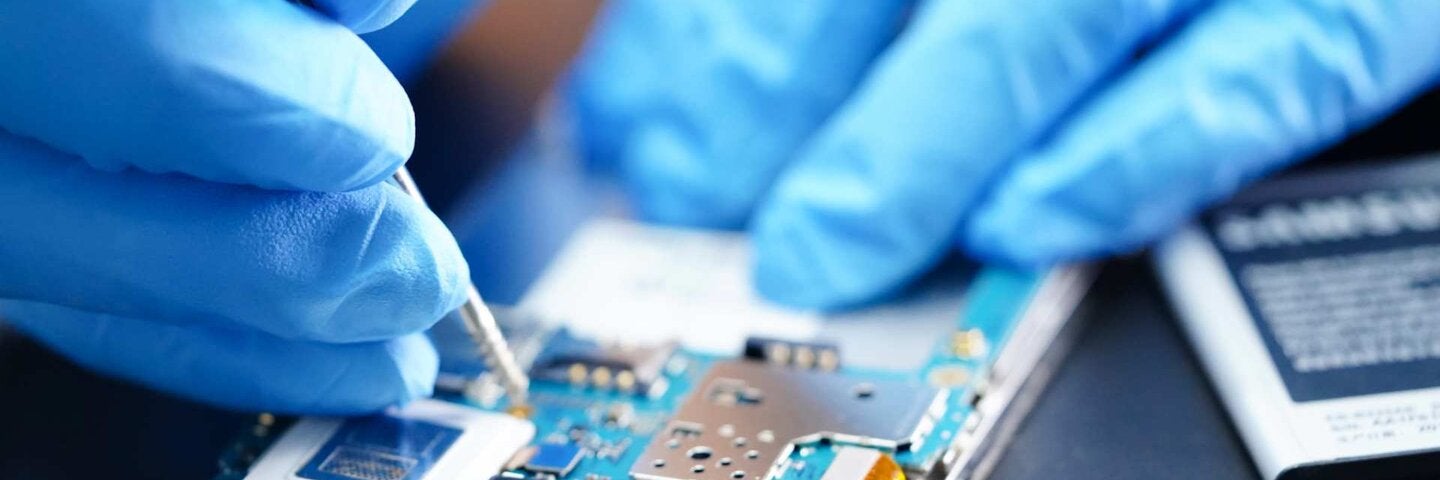
This course will teach you how to design printed circuit assemblies & enclosures for EMI-EMC compliance including IOT and 5G. This course will be held virtually via Adobe Connect.
Get More Info
What you can learn.
About This Course
Who Should Attend:
- Digital logic engineers
- System architects, EMC specialists
- Technicians, PCB layout professionals
- IC designers, IC package designers
- Application engineers
- Anyone who works with high-speed digital logic
- Anyone who works with any digital logic implemented in the submicron processes that are becoming standard in the industry
- Engineering managers
- Project managers
Topics Covered:
Fundamentals – Frequency, Time, and Distance Lumped Versus Distributed Systems Four Kinds of Reactance Ordinary and Mutual Capacitance & Inductance
EM Fields – Geometry, C, L, & Zo interrelationships C & L Resonance EMI, Source, path, and receptor. Why all three must be present to have an EMI problem.
EMI regulations – standards for the USA, Europe (EU), and Asia. The course text provides a detailed description of all the test requirements, equipment to conduct the tests and the governing bodies/committees that mandate the tests. Threats – RFI, ESD, Power Disturbances, Internal EMI Issues – Frequency, Amplitude, Time, Impedance Dimensions
EMI Requirements– Commercial, Military, Avionics, Automotive, Medical, Communications
Conducting an EMI Test – Pre-compliance, Compliance Testing, and Post-Audit Testing. What is uncertainty and how does it affect the test plan?
How the Tests Are Conducted—For all the following tests, the hardware instrumentation, the layout, the pass/fail criteria, and tips/techniques to pass the test will be covered. Also, the test site will be defined, i.e. OATS, screen room, anechoic chamber, and TEM cell. The step-by-step sequence of how each test is conducted will be detailed.
- Conducted Emissions
- Radiated Emissions
- RF Immunity Conducted RF Immunity
- ESD
- Lightening
- Electrical Fast Transient
- Shock and EMP
Interference Coupling Mechanism – What are the near/far field, coupling modes, resonance and why are parts placement, proper terminations and grounding so important for PCBs.
RFI, EMI regarding PCBs, computers, analog designs, and systems
Grounding designs/Filtering – Single ground, modified and multipoint grounding, which one should be used for your design.
CM Radiation – Why is common mode (CM) the major problem versus differential mode (DM)? Antenna Loops – Why are antenna loops the major cause of radiated emission failures for PCBs?
Basics of PCB Radiation – Why do both lumped and distributive transmission lines (T.L.) circuits radiate? Why does a high Q circuit radiate? How do you terminate a T.L. to minimize radiation? What about the capacitive load and why does it cause radiation?
PCB Suppression Techniques – Terminations, filters, and devices – how are they used to suppress radiation?
Design for Immunity – Watchdog timers, offensive/defensive programming, checksum, Hamming, and other techniques. How intelligent software helps pass immunity testing.
Switching Mode Power Supplies (SMPS) – SMPS Chopping Frequency.
- Why is it the major cause of conducted emissions?
- Filters – Schematic configurations of harmonic filters.
- What happens when transients/ESD hits the SMPS mains?
- What are the immunity concerns?
- What are screens and snubbers, and how it a transformer wound?
Crosstalk – Inductive/capacitive, forward/backward – How does it occur? Why does it cause radiation and how is it minimized? How to minimize PCB antenna loops. Do vias cause radiation?
Power/Ground Planes – Splits, slots, moats, floats, drawbridge, how to design for minimizing emissions from power/ground planes.
How to design for digital/analog (multibias) and single bias PCBs
Picket fences, the 20H rule, and Cu fills – What can they do to suppress emissions?
Ideal stackups to be EMC
Spread Spectrum Clocking – Why does it suppress radiated emissions? Under what conditions can it be used? Is there a better method?
Bypass and Radiation on PCBs – Why use the 0201, Ycap and four terminal cap? Types of innerplane capacitance and does innerplane capacitance help with emissions?
Interference Coupling Modes – Why does ground bounce cause differential and common mode noise and how does that cause emissions?
Near/Far Field – What determines the breakpoint between them and what happens to the characteristic impedance at the breakpoint?
Differential/common coupling modes and resonance – What are the quarter length resonant mode differences when the load impedance is very high versus very low?
Analog circuitry – Transients, filtering, grounding, and noise isolation. Opto couplers versus spin resistors; which is better?
Cables/Connectors and PCB, Concerns of PCBs Interfacing with Filtering and Shielding
Capacitive and Magnetic Shielding – What is the difference and how should the shield be tied to the PCB ground for either case?
Slots in PCBs – Why do they radiate and is the radiation through them predictable?
Shield Grounding – How should shields be tied to the PCB ground to minimize circulation current?
Cable Radiation – Radiation through the shield and at the PCB connector bulkhead connection.
Shielding Types – When do we use Cu and Al versus mu metal, steel, or permalloy?
Transfer Impedance – What is it? Why is it detrimental to shielding, and how is it minimized?
Shielding Connection – Leakage – How to design a non-emission connection of a PCB connector to a bulkhead.
Enclosures, Motherboards, backplanes & blades
Loss of PCB Ground Plane in Cables – Why does it cause crosstalk, radiation, reflections, and propagation delay?
How to design a PCB land trace to a connector pin to eliminate reflections. Demo of an actual design.
Cables Configuration – What shielding/grounding techniques should be used to minimize crosstalk and radiation when a PCB is connected to a cable?
Antenna Loops with Cable Connections – Why do shielding pigtails cause emission non-compliance?
High-Speed Connectors – How are they configured to minimize skin effect, dielectric loss, crosstalk, and radiation?
Filtering – Types of filters, their attenuation capability and how should they be mounted?
Shielding vs Filtering – Cost tradeoffs versus attenuation capability –When should either or be used?
Using Ferrites – Amperes Rule – Why do they work so well for both DM and CM?
Filtering Mains Supply – Using capacitors, chokes, and torroids. Filtering both DM and CM noise.
Using Transients Suppressors on Mains and I/O lines – Where should TVSSs, Spark Gaps, Varistors, and Zeners be used. Radiation Through Shields – Current density versus skin depth, incident versus reflected fields
Effects of source and load impedance and why mismatches cause radiation
The capacitive load: Zo and propagation delay and radiation effects
90o, 45o bends: Are they radiation concerns?
Guard traces: Do they stop crosstalk; can they resonate?
Interplane capacitance: how thin, what material and stack-up placement?
Why the 0201: both for better bypassing and EMI control
Via discontinuity and via resonance concerns
Buses – An explanation of design techniques to minimize radiation for the following buss structures:
- Multidrop systems, drivers, transceivers, and designing a high-speed bus
- How they function, clock rates, typical failures
- ISI: minimize the effect with equalization and pre-emphasis
- LVDS: types, unbalance, noise, layout, and making them function
Attributes/drawbacks of loosely/tightly couple differential pairs
Differential impedance: odd and even modes and why odd mode leads to radiation
Advantages and disadvantages of edge (side by side), broadside (dual), asymmetric, and microstrip differentials
Internet of Things (IOT) – How to provide shielding and grounding for cable assemblies when interfacing with various devices (auto, telecom, etc.), high speed and high/low voltages.
Design Techniques for providing radiation and susceptibility compliance for 5G (24 Gbs to 54 Gbs). Methods described will be pre-emphasis on drivers and how to pass radiated emission on double amplitude and high edge rate signals. Interfacing high-speed connectors for reflections and radiation.
One big concern today is the aperture openings versus the frequency of signals versus the higher density packaging, i.e. ICs are running hotter and the ever-increasing signal edge rate. This leads to more radiation through the apertures, i.e. lamda is shorter, but more heat is generated because Power = C times F times V2.
What’s new in enclosure absorption materials and what are their capabilities for minimizing radiation? What’s new in heat sink materials (backplanes, blades, servers) which in turn alleviate the need for heat conduction through the apertures? These current issues will also be covered in the course.
Robert Hanson, MSEE, has unmatched experience in teaching and knowledge of electronics. As a Testability Overseer for Boeing CommercialAirline products, Mr. Hanson has worked with non-EEs and EEs. He understands the need to use clear communication, and he spends extra time answering student questions during his presentations or privately afterward. Mr. Hanson has over 40 years of experience in the design manufacturing and testing areas. His initial education was in Industrial Engineering (BSIE) Business Administration (BSBA). After receiving his BSEE/MSEE, he became highly involved in all aspects of electronic testing. As a digital design engineer at The Boeing Company, Rockwell, Honeywell, and Loral.
Mr. Hanson designed and provided prototype operational analysis on many high-speed designs, including PCBs for AWACs, B1-B, 747-400, missiles, and ground support test equipment. He has played a very active role in automating the line, implementing robotics, and participating in producibility studies and working in the CAE/CAD/CAT, JIT, simulation, and automatic assembly environments. He has also performed studies and headed research projects in the computer-integrated manufacturing environment. Mr. Hanson has extensive experience in the testing disciplines (both factory and field,commercial and military as the testability overseer for Boeing Commercial Airline products.
Building on that practical knowledge, Mr. Hanson has taught these courses many times receiving outstanding reviews each time from participants. He has presented his courses for the University of California – Berkeley, University of Wisconsin, University of Oxford (England), Seattle Pacific University, University of Washington, University of California – Los Angeles. Mr. Hanson has taught electronic courses throughout the United States, Europe, South Africa, the Middle East, and Asia.
AWARDS: Boeing Company Aerospace Man of the Year for saving $6,000,000 for inventing a new testing technique for the Boeing B-1 bomber electronics.
Robert Hanson has conducted private seminars and/or consulting for 3-Com, Advanced Fibre Communications, Alcatel, Allied Signal, AMO, AMO-Dresden, Apple, AT&T, Autoliv, Boeing, Chrysler, Cisco, Compaq, Cray, da Vinci Systems, Data Device, Dell, Delphi, EDA Technologies – South Africa, Ford, Free Scale Technologies, Gateway, GE, GenRad, Honeywell, HP, HP – Barcelona, IBM, Intel, Kaneta High Tech Materials, KLA Tencor, Lockheed, Lucent, LXE, Marconi, Micron, Motorola, NASA, NEC, eLuminant, Navico, Nortel, Northrop Grumman, Panasonic, Qualcomm, Raytheon, Rockwell, Samsung-Korea, Solectron, Storage Tek, Sun, Tektronix, Teradyne, Texas Instruments, TRW, Tyco Electronics, Tycom Laboratories, U.S. Trade Commission, United Defense, Wilson-Sonsini-Goodrich and roseti Law Firm, Xerox, and Xilinx.
ABT Media – Singapore, Advanced Electronic Diagnosis (AED) – Saudi Arabia, Atkins Technical, Inc., Bacharach Inc. BBN Graphics, Benthos, Bourns, Compression Labs, Inc. Con Med Linvatec, Goutier, Delphax, Dynalco, Eldec, First Inertial Switch, Fluke, Genicom, Hathaway, Johnson&Johnson, Jet Propulsion Labs (JPL), Loral Aerospace, Martin Marietta, Maxim Integrated Products, McBeth, Medrad, Medtronic, Motion Engineering, Inc., Norsat International, Okidata, Pharmacia Deltec, Precor, Satcom, Southern Research Institute, Wellex, Aesalsan (Turkey), Jefferson Labs, Schmitt, NVE, McDermott, Will, and Emery Law Firm, FLIR, Data 1/0, Pulsecom, Symbol Technologies, U.S. Navy – Idaho, and JSI.
Each Student Receives:
- A 310-page comprehensive set of course notes
- “EMC for Product Designers” (Fifth Edition) by Tim Williams
- A 26-page “How to Become a Circuit Master,” a booklet that provides a detailed description of how a bareboard is manufactured and tested
A supplemental addendum reinforcing information in the course notes is included.